
When "Clean" Assemblies Still Fail: Inside a Real Failure Investigation
Not every electronics failure has an obvious cause.
Sometimes the assembly passes inspection. It passes cleanliness testing. It performs exactly as expected during manufacturing—and then, months later, warranty claims begin to appear.
That was the situation Foresite recently investigated.
A customer began experiencing fractured solder joints beneath bottom-terminated components (BTCs) operating in sealed systems. At first glance, the failures looked mechanical. But as the investigation unfolded, the evidence revealed a much more complex story—one involving trapped no-clean flux, silicone outgassing, and an interaction that traditional cleanliness testing alone couldn't explain.
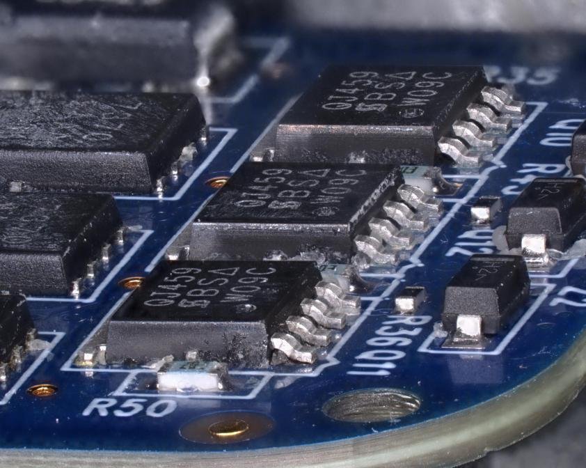
Initial field observations showed fractured SMT components with residue appearing beneath low-standoff packages.
The First Set of Clues
The returned assemblies shared several unusual characteristics.
Multiple SMT components showed fractured solder joints, but the residue wasn't appearing around exposed leads. Instead, a soft, flux-like material was extruding from beneath the component body.
That immediately raised an important question: if this was simply leftover assembly residue, why was it only appearing beneath certain components—and why were neighboring components unaffected?
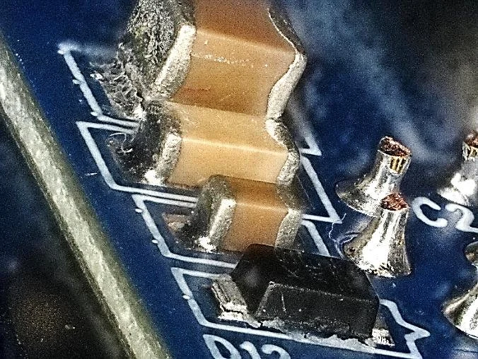
Not all components failed equally. Areas with trapped flux beneath low-standoff components showed fractures, while adjacent components remained intact.
Rather than assuming contamination was responsible, Foresite approached the failure the same way investigators approach any complex problem: check out the most likely explanations first.
Clue #1: Was It a Cleanliness Problem?
The first step was Ion Chromatography (IC) and C3 testing. Surprisingly, the assemblies met accepted cleanliness standards. By traditional measurements, there was no indication of harmful ionic contamination that would explain the field failures.
This ruled the obvious suspect out.
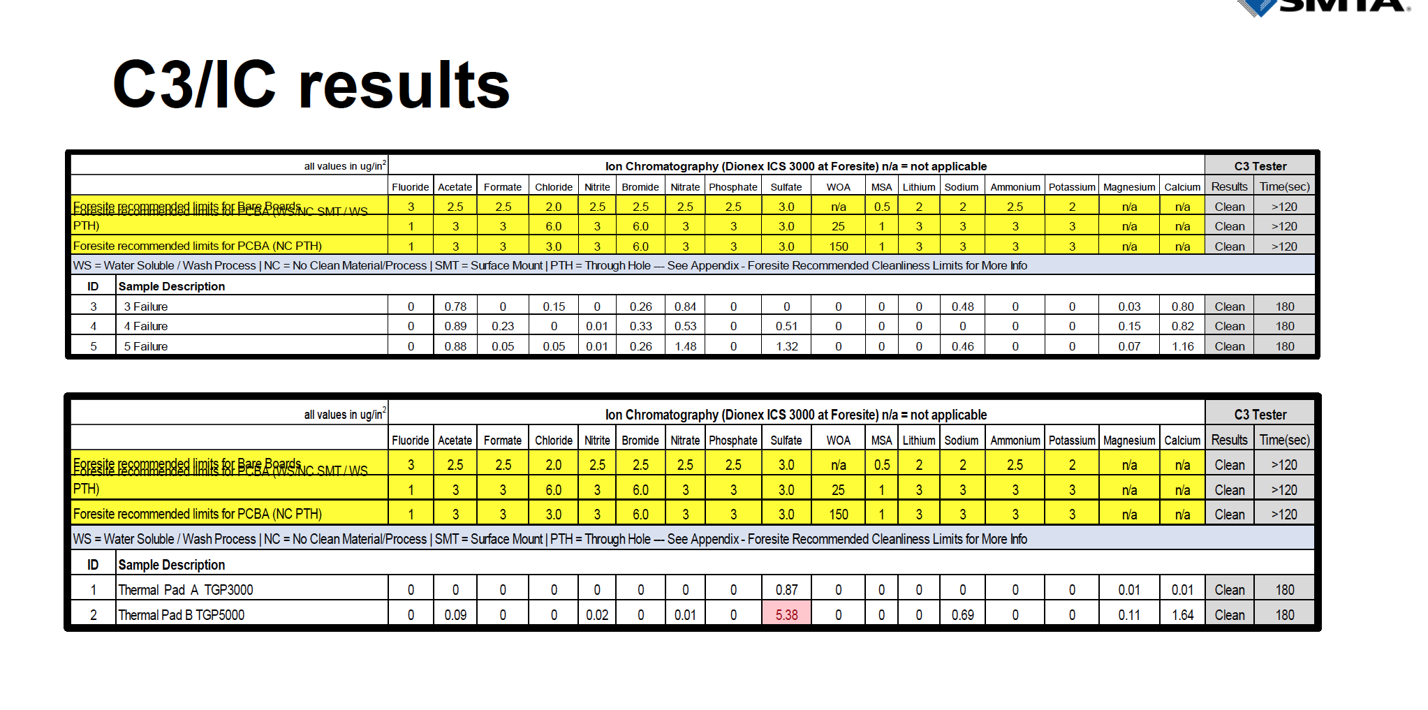
Conventional cleanliness testing classified the assemblies as clean, forcing investigators to look beyond traditional contamination mechanisms.
Clue #2: The Residue Had a Story to Tell
Attention shifted to the mysterious material protruding from beneath the failed components.
Using Fourier Transform Infrared Spectroscopy (FTIR), Foresite compared the chemical fingerprint of the extruded material against known materials used during assembly.
The results showed strong similarities between the residue, the original no-clean flux, and nearby silicone thermal interface materials. Rather than being random contamination, the residue appeared to be the product of an interaction between materials already present inside the assembly.
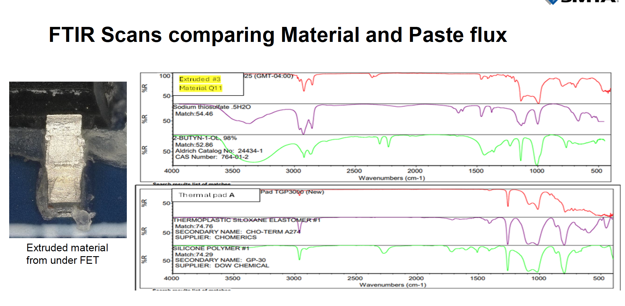
FTIR analysis linked the extruded material to both the original no-clean flux and the silicone thermal interface material.
Clue #3: The Force Was Coming From Below
The next question was mechanical: why were the solder joints actually breaking?
Cross-sectional analysis revealed something unexpected.
Rather than failing from normal solder fatigue, components had separated from the PCB because a hard material had formed beneath them. That expanding layer was physically pushing upward against the component body, creating enough vertical force to fracture the solder joints.
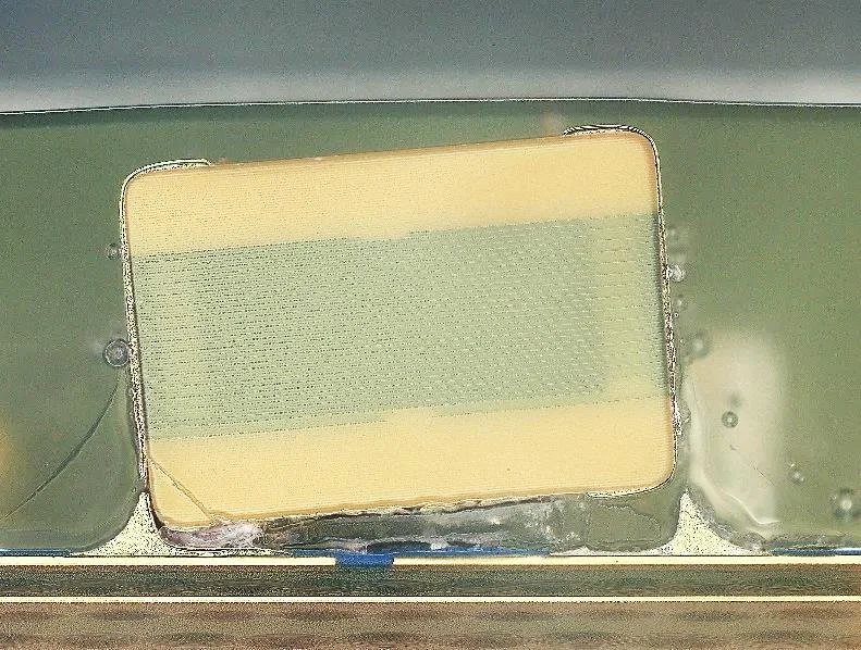
Cross-sectional analysis revealed a hard material beneath the component, producing the upward force responsible for the fractured solder joint.
Clue #4: The Chemistry Confirmed the Theory
One final question remained: what exactly was that material?
SEM/EDS elemental analysis revealed a high concentration of silicon within the extruded residue.
That finding connected the final pieces of evidence, confirming an interaction between trapped no-clean flux and silicone thermal interface materials inside the sealed assembly.
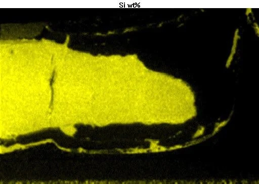
SEM/EDS analysis identified a silicon-rich material beneath the component, confirming the interaction between trapped flux residue and silicone outgassing.
The Breakthrough
When viewed individually, none of the findings fully explained the failures:
Cleanliness testing indicated the assemblies were clean.
FTIR identified similarities between the residue and known assembly materials.
Cross-sectional analysis revealed an upward mechanical force.
SEM/EDS identified silicon concentrated within the expanding material.
Together, however, those pieces told the complete story.
Trapped no-clean flux beneath low-standoff components gradually interacted with compounds released from nearby silicone thermal pads inside the operating environment. Over time, that reaction produced an expanding material that physically lifted the components and fractured the solder joints.
This wasn't a manufacturing defect in the traditional sense. It was a long-term interaction between assembly materials and the operational environment—one that only became apparent through a comprehensive failure analysis.
What the Investigation Revealed
This investigation highlights an important lesson for electronics manufacturers: passing conventional cleanliness testing doesn't always guarantee long-term reliability.
Some failure mechanisms only emerge when materials interact over months of real-world operation.
By combining multiple analytical techniques and following the evidence instead of assumptions, Foresite was able to identify the true root cause and provide actionable recommendations for reducing future failures.
When unexplained field failures occur, solving the problem often requires looking beyond a single test. Sometimes, it also requires a full investigation and deeper understanding of how materials behave throughout the life of the product.